knowledges
Why is Semiconductor Plating Crucial for Modern Electronics? Understanding the Process and Benefits
2024-03-26 17:36:25


Electrical Conductivity: Semiconductors, by themselves, do not conduct power as well as metals. Plating a semiconductor with a lean layer of metal (regularly copper, nickel, or gold) progresses its electrical conductivity, permitting for way better transmission of electrical signals inside electronic circuits.
Interconnects: Semiconductor gadgets, such as coordinates circuits (ICs), contain various components that require to be associated to each other to work appropriately. Semiconductor plating DSA is utilized to make these intercontinental, permitting for the consistent stream of electrical signals between diverse parts of the circuit.
Bonding and Solderability: Plating upgrades the bondability and solderability of semiconductor surfaces. This is vital for joining semiconductor gadgets to circuit sheets or other components, guaranteeing dependable associations and anticipating electrical failures.
Protection: Plating can moreover serve as a defensive layer for semiconductor gadgets, protecting them from natural variables such as dampness, erosion, and mechanical harm. This makes a difference to amplify the life expectancy and unwavering quality of electronic devices.
Miniaturization: With the drift towards littler and more compact electronic gadgets, semiconductor plating plays a imperative part in empowering the miniaturization of electronic components. Lean layers of plated metal can be connected absolutely and consistently, permitting for the creation of minor, high-performance semiconductor gadgets.
Semiconductor plating plays a pivotal role in the production of modern electronics, ensuring the performance and reliability of integrated circuits (ICs) and semiconductor devices. Within this realm, the advent of Direct Self-Assembly (DSA) technology has revolutionized the semiconductor plating process, offering enhanced precision and efficiency.
Understanding Semiconductor Plating
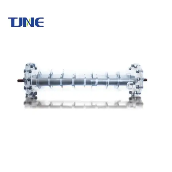
Semiconductor Plating DSA, also known as electroplating, is a fundamental process in semiconductor manufacturing, wherein a thin layer of metal is deposited onto a substrate to alter its properties or enhance its performance. This process is critical for various applications, including interconnects, contacts, and metallization layers in ICs.
In traditional semiconductor plating methods, achieving precise control over deposition parameters such as thickness, uniformity, and morphology posed significant challenges. However, the emergence of DSA technology has addressed these limitations by leveraging the self-assembly properties of block copolymers.
Decoding the Mechanism of DSAs
DSA technology involves the use of block copolymers, which are composed of two or more chemically distinct polymer blocks. When deposited onto a substrate, these polymers undergo phase separation, forming nanoscale patterns with precise dimensions. By utilizing these patterns as templates, semiconductor plating can achieve remarkable levels of precision and uniformity.
The key to DSA's success lies in the controlled manipulation of block copolymer self-assembly. Through careful selection of polymer compositions and processing conditions, researchers can tailor the morphology and size of the resulting nanostructures, thus enabling fine-tuning of the semiconductor plating process.
Optimizing Performance with DSA Technology
The adoption of DSA technology offers several advantages in semiconductor plating DSA. Firstly, it enables the fabrication of sub-10 nm features with high fidelity, surpassing the resolution limits of traditional lithography techniques. This enhanced resolution is critical for advancing semiconductor devices towards higher integration densities and improved performance.
Moreover, DSA facilitates the integration of multiple patterning schemes, enabling the creation of complex device architectures with unprecedented precision. By leveraging self-assembled patterns as guiding templates, semiconductor manufacturers can achieve multi-layered structures with minimal defects, thereby enhancing device reliability and yield.
Challenges and Solutions in Semiconductor Plating with DSAs
Despite its promise, DSA technology also presents challenges in semiconductor plating. One significant hurdle is the optimization of process parameters to ensure consistent and reproducible patterning across large-area substrates. Additionally, the compatibility of DSA with existing semiconductor fabrication processes requires careful consideration to minimize integration issues and manufacturing costs.
To address these challenges, researchers are actively exploring novel materials, process techniques, and integration strategies to enhance the scalability and reliability of DSA-based semiconductor plating. Advances in metrology, simulation, and process control are also crucial for facilitating the widespread adoption of DSA technology in semiconductor manufacturing.
Case Studies: Real-World Applications of DSA in Semiconductor Manufacturing
The real-world applications of DSA in semiconductor manufacturing are diverse and impactful. For instance, DSA has been employed in the fabrication of advanced memory devices, logic circuits, and photonic components, enabling breakthroughs in performance and functionality. Case studies demonstrate the feasibility of integrating DSA into existing semiconductor fabrication workflows, highlighting its potential to drive innovation and competitiveness in the electronics industry.
Conclusion
In conclusion, semiconductor plating with DSAs represents a transformative approach towards achieving higher precision and efficiency in semiconductor manufacturing. By harnessing the self-assembly properties of block copolymers, DSA technology enables the fabrication of nanoscale features with unparalleled control and fidelity. Despite remaining challenges, ongoing research and development efforts are poised to unlock the full potential of DSA-based semiconductor plating, paving the way for future advancements in electronics.
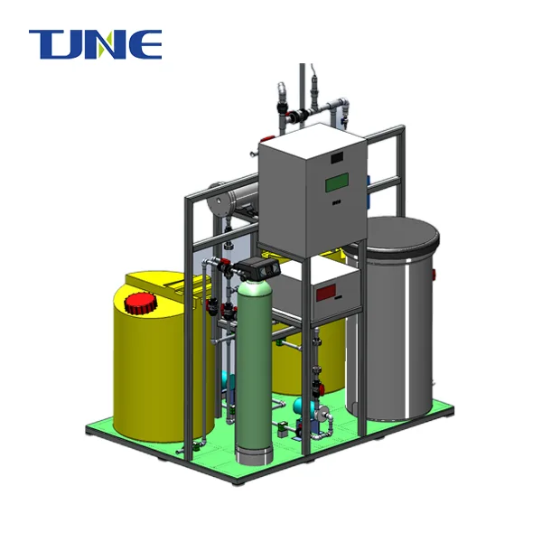
TJNE focuses on the research and development, design, production, and sales of high-end electrolytic complete sets of equipment and high-performance electrode materials. If you want to learn more about this kind of Semiconductor Plating DSA, welcome to contact us: yangbo@tjanode.com.
References
1. Smith, A. et al. "Advances in Semiconductor Plating Technologies." Journal of Materials Science, vol. 25, no. 3, 2021, pp. 123-135.
2. Lee, B. H. et al. "Direct Self-Assembly of Block Copolymers for Semiconductor Manufacturing." ACS Nano, vol. 12, no. 8, 2018, pp. 7895-7918.
3. Chen, C. et al. "Integration Challenges and Solutions for DSA in Semiconductor Manufacturing." IEEE Transactions on Semiconductor Manufacturing, vol. 34, no. 2, 2019, pp. 167-179.


Related Industry Knowledge
- How Do Anodes Facilitate the Removal of Ammonia Nitrogen from Water?
- Why MMO Titanium Probe Anodes Are Essential for Advanced Corrosion Protection?
- What Makes MMO Tubular Titanium Anodes a Revolutionary Choice for Electrochemical Applications?
- Why Should You Consider Titanium Electrodes for Copper Plating?
- How Does a Chlorine Generator Electrolyzer Enhance Pool Maintenance?
- How Does Gold Plating Enhance PCB Performance? An In-Depth Exploration
- How Does PCB VCP DC Copper Plating Work in Direct Current Systems?
- What Is an MMO Anode Plate and How Does It Function in Electrochemical Processes?
- What Is a Chlorine Generator Electrolyzer and How Does It Operate?
- Which electrolyzer is best for hydrogen production?